From Ars Technica · · 1 min
Chip Giants Unite Around ASML’s $400M Next-Gen Lithography
TSMC, Samsung, and Intel are adopting high NA EUV and a new photomask standard to dramatically boost future chip production.
In brief
TSMC, Samsung, and Intel are adopting high NA EUV and a new photomask standard to dramatically boost future chip production. The semiconductor industry is uniting around ASML's $400M high NA EUV machines and 12-inch photomasks to power the next decade of AI hardware. Originally reported by Ars Technica.
Chip giants embrace $400M machines
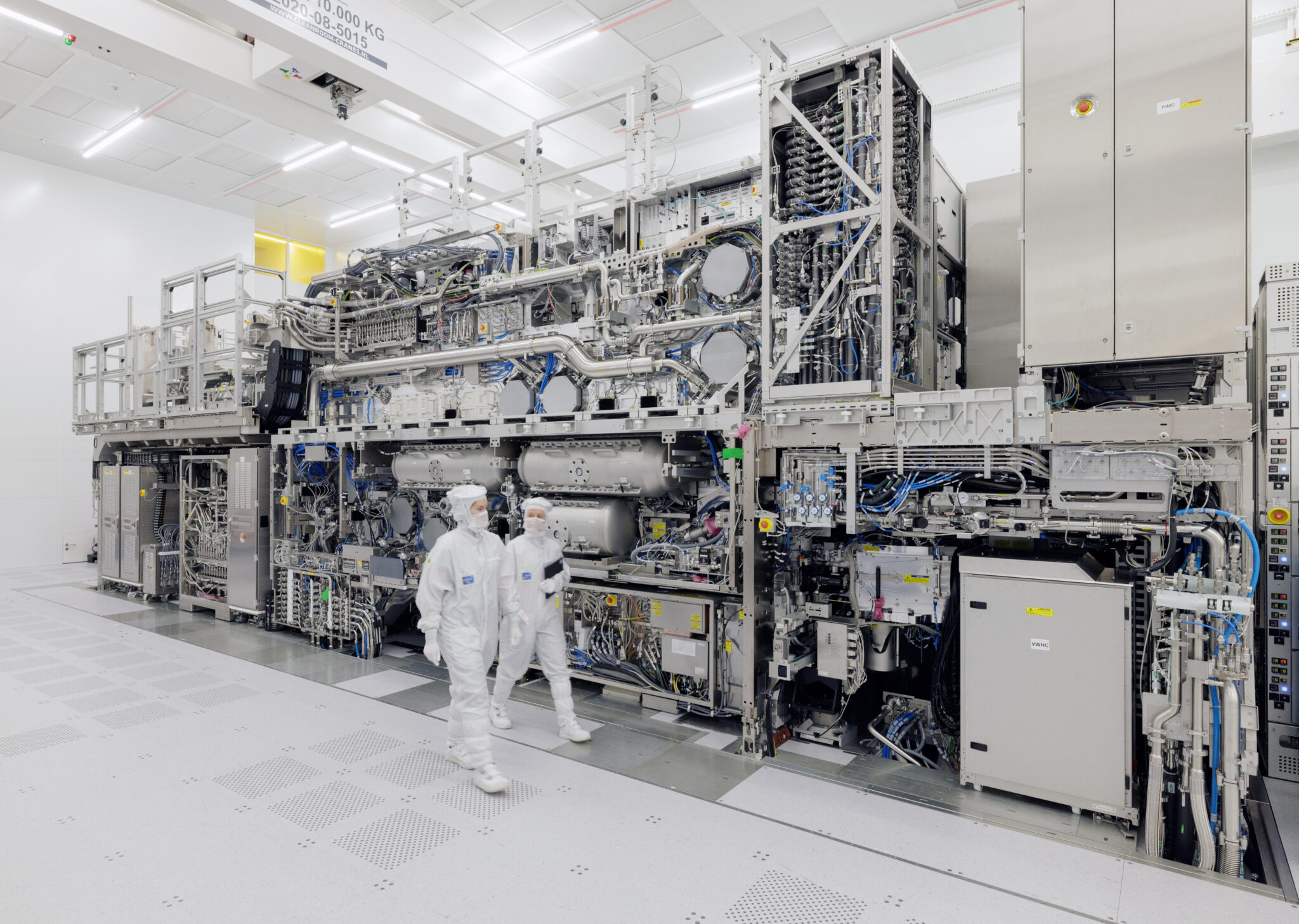
Samsung and TSMC have joined Intel in adopting ASML’s high-numerical-aperture EUV lithography tools. The move secures ASML's monopoly on the ultra-expensive machinery needed for next-gen silicon.
“Leading chipmakers Samsung Electronics and Taiwan Semiconductor Manufacturing Co. announced plans to adopt ASML’s latest chipmaking machines...”
Harnessing extreme light and plasma
High NA EUV machines continuously zap molten tin with lasers to generate 200,000°C plasma. Massive, precise mirrors then reflect short-wavelength light to etch microscopic circuits onto silicon wafers.
“...continually zapping molten tin into plasma with temperatures around 200,000° C, along with mirrors collecting light from the plasma...”
A staggered rollout schedule
Intel is already running high NA EUV tools in high-volume production for 2026 mobile processors. Samsung and SK Hynix plan to produce memory chips with it by 2028, while TSMC targets 2030 for advanced logic.
“The US company has used the technology in high-volume manufacturing of Panther Lake processors for mobile computing devices starting in July 2026.”
The 12-inch photomask shift
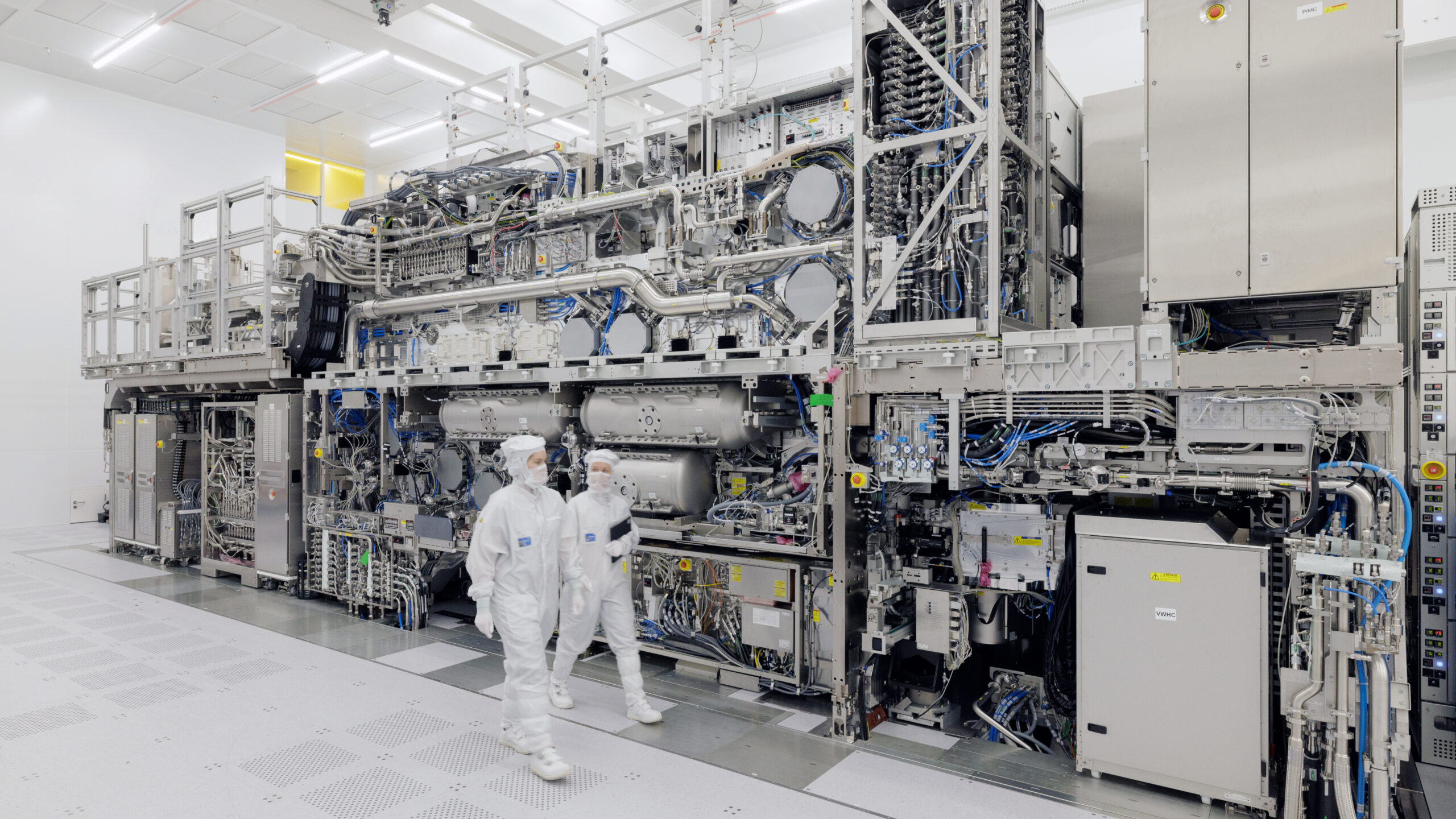
To maximize output on these massive machines, chipmakers agreed to double the stencil size from 6-inch to 12-inch photomasks. This standard change could boost productivity by up to 40 percent.
“That shift could eventually improve the chipmaking productivity of high NA EUV machines by 40 percent...”
Driven by the AI boom
Rapid construction of AI data centers has created global memory shortages, driving up consumer tech prices. Maximizing lithography output is now essential to keep pace with demand.
“Tech companies’ rush to construct new AI data centers has also contributed to a global shortage of memory chips...”
China faces a 15-year gap
Western export controls prevent ASML from selling advanced EUV tools to Chinese firms. Industry experts estimate China will need at least 15 years to develop a homegrown EUV supply chain.
“An executive at Germany’s Zeiss Group... recently predicted that China would need 15 years to develop EUV lithography machines.”
Here's the gist
The semiconductor industry is uniting around ASML's $400M high NA EUV machines and 12-inch photomasks to power the next decade of AI hardware.